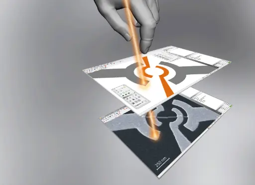
Nanofabrication and lithography
Lithography and nanofabrication is used to produce micro and nano scale devices for a wide variety of applications such as biosensors, waveguides, micro electromechanical systems (MEMS) and microfluidics. A combination of lithography, deposition and etching can create all kinds of intricate structures.
We help with designing, patterning and fabricating your devices for rapid prototyping and proof-of-principle development. Our advanced range of lithography and nanofabrication tools can produce anything from thin film transistors to lab-on-a-chip systems.
Electron beam lithography
Overcome the diffraction limit to produce nano-scale features. Small feature sizes maximise substrate use, and often correlate with high power efficiency and high operating frequency for your devices.
Optical lithography
Full wafer UV illumination through a mask for fast, repeatable exposures, or use direct write laser lithography for rapid prototyping.
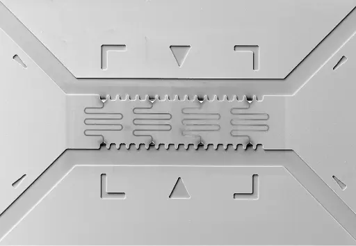
Device fabrication is achieved using a variety of deposition methods capable of processing any material you need. Structures are defined using the lift-off process or etching.
- Magnetron sputtering, both RF and DC.
- Thermal evaporation.
- Reactive ion etching, and deep reactive ion etching.
- Wet etching.