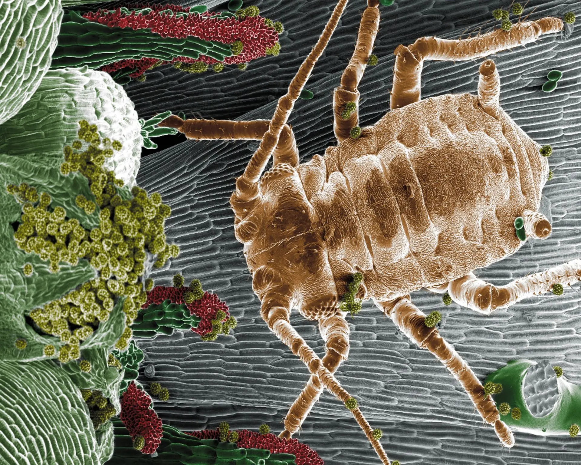
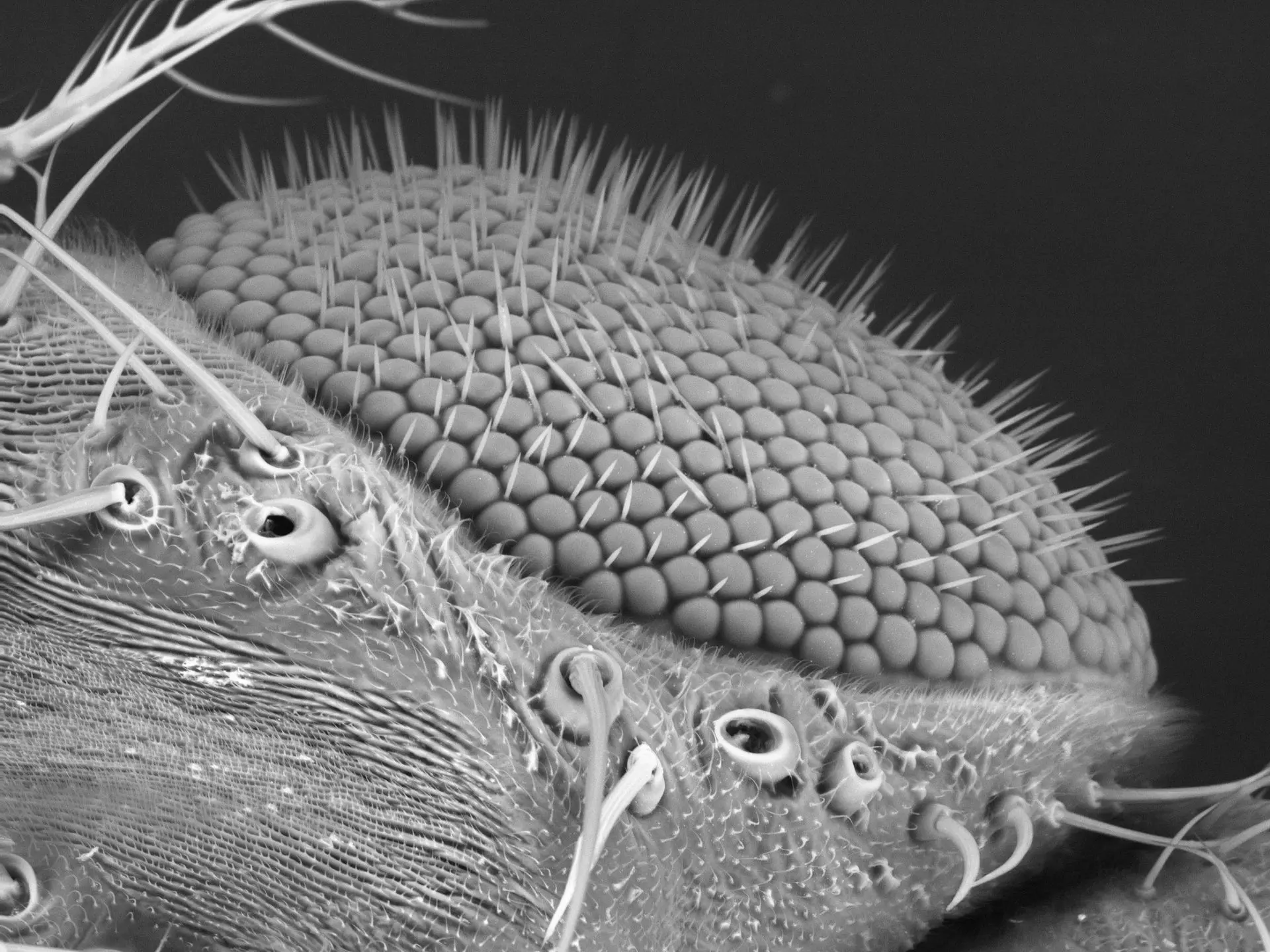
Electron Microscopy
Electron microscopy provides single-nanometer resolution imaging for the ultimate level of detail. Whether you’re interested in the internal structure of cells or nano-electronic devices, electron microscopy will give you direct visual characterisation of the smallest structures.
We have a range of electron microscopes suitable for anything from high-throughput quality control to in-depth failure analysis and high resolution R&D. Our flexible approach means we can mix-and-match our instrumentation to meet your requirements.
Scanning electron microscopy
Scanning electron microscopes (SEMs) are used to image the sample surface at up to 500,000X magnification. We have a range of SEMs equipped with a variety of detectors to give a wealth of supporting information.
- Thermal field emission (TFE) for better than 10 nanometer resolution.
- Secondary Electron (SE) and InLens detector for high resolution surface-sensitive imaging.
- 4-quarter Backscatter electron detector (BSD) for contrast from different materials.
- Electron Backscatter Diffraction (EBSD) for grain orientation mapping and quantitative crystallography.
- Scanning Transmission Electron Microscopy detector (STEM) for imaging electron-transparent samples and nanoparticles. Read our nanoparticle case study to find out more.
- Energy-Dispersive X-ray spectroscopy (EDX) for qualitative and quantitative elemental composition analysis, including point ID and mapping. Read more about elemental characterisation with EDX here.
Sample preparation
We have a full suite of sample preparation equipment for all kinds of samples, from biological specimens to electronics and metallography.
- Sputter coating of carbon, gold or palladium to improve the resolution of non-conductive samples.
- Ultra-microtome, resin embedding and sectioning between 30 – 100 nanometers thick for TEM samples.
- Grinding and polishing for surface preparation of SEM samples and thinning of TEM samples.
- Alpha Plasma AL-18 for oxygen/argon plasma cleaning and decapsulation.
- Optical microscopy for finding the area of interest and evaluating sample preparation.